
Paper: 2605.30345 Authors: Qinpei Luo, Ruichun Ma, Xinyu Zhang, Lili Qiu Categories: cs.AI, cs.CL, cs.LG
The Gap
Generative AI has automated IC design (chips), but PCB schematic design (the boards that connect chips) remains manual. Prior work focused on layout optimization or component placement given an existing schematic. No one tackled generating the schematic itself from natural language because existing formats (KiCad, Altium) are verbose XML/JSON with absolute coordinates and tool-specific syntax — LLMs drown in geometric noise and can’t reliably generate valid schematics.
Problem: PCB design manual + expertise-intensive
   |
   v
Gap: Existing formats = geometry-heavy + tool-specific
   |                    (X=142.5, Y=87.3, rotation=90...)
   v
Assumption: LLMs need semantic primitives, not coordinates
   |
   v
Method: New representation = editing operations + relative placement
   |                          (place R1 right-of U1, wire R1.pin2 to U1.GND)
   v
Evidence: SchGen outperforms baselines on wire accuracy + functional correctness
   |
   v
Conclusion: Representation design > model scale for hardware generation
The Increment
One sentence: Before — PCB schematics locked in geometry-heavy formats, inaccessible to LLMs; After — semantic code representation enables LLM-driven schematic generation from natural language.
Core Mechanism
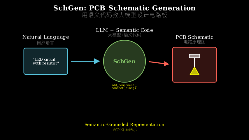
SchGen’s representation has three layers. First, component instantiation declares parts with semantic names (not coordinates): U1 = MCU("STM32F4"). Second, relative placement positions components using spatial relations: place(R1, right_of=U1, offset=2). Third, pin-name wiring connects components by function, not geometry: wire(R1.pin2, U1.GND). This transforms schematic generation from “predict X/Y coordinates” into “predict which components connect and how.”
Input: "Add LED indicator to microcontroller"
   |
   v
[Component Layer]  U1=MCU, LED1=LED, R1=Resistor
   |
   v
[Placement Layer]  place(LED1, above=U1)
   |               place(R1, between=[U1, LED1])
   v
[Wiring Layer]     wire(U1.GPIO_PIN, R1.pin1)
   |               wire(R1.pin2, LED1.anode)
   v               wire(LED1.cathode, U1.GND)
Output: Executable schematic code
Think of it like cooking instructions vs. a photograph of a dish. Traditional formats are the photograph — they show where every ingredient ended up (X=5cm, Y=3cm), but you can’t recreate the dish from pixel coordinates. SchGen’s representation is the recipe — it tells you the steps (add resistor, place it near the chip, connect pin 2 to ground). The recipe is executable: a renderer can turn it into any visual format. More importantly, an LLM can learn to write recipes because they follow semantic logic (resistors limit current, so they go between power sources and LEDs), not arbitrary geometry.
Key Concepts
-
Semantic grounding: Instead of treating schematics as drawings (lines at coordinates), treat them as functional relationships (this resistor limits current to that LED). Pin names like
GPIO_PINandGNDcarry meaning; coordinates like(142.5, 87.3)don’t. When you wireR1.pin2toU1.GND, you’re expressing intent (connect resistor to ground), not geometry. This lets the LLM reason about electrical function rather than memorize spatial patterns. Example: “Add pull-up resistor” becomesR1=Resistor(10k); wire(R1.pin1, U1.VCC); wire(R1.pin2, U1.INPUT)— the model understands pull-ups connect between power and signal, not because it saw this X/Y pattern before. -
Relative placement: Absolute coordinates are brittle (move one component, everything breaks). Relative placement uses spatial relations:
right_of,above,between. This mirrors how humans think (“put the capacitor near the power pin”) and makes schematics robust to layout changes. The renderer resolves relations into coordinates, but the LLM never sees them. Example:place(C1, near=U1.VCC, offset=1)works regardless of where U1 ends up on the canvas.
Framework Shift
Before (geometry-driven):              After (semantics-driven):

User: "Add LED"                        User: "Add LED"
   |                                      |
   v                                      v
LLM generates:                         LLM generates:
<component id="LED1"                   LED1 = LED("red")
 x="142.5" y="87.3"                    place(LED1, above=U1)
 rotation="90">                        R1 = Resistor("330")
<wire x1="142.5" y1="87.3"            place(R1, between=[U1,LED1])
      x2="98.2" y2="65.1"/>            wire(U1.GPIO, R1.pin1)
                                       wire(R1.pin2, LED1.anode)
Problem: Coordinates are              wire(LED1.cathode, U1.GND)
arbitrary, no semantic check
                                       Benefit: Semantically valid,
                                       renderer handles geometry
[One sentence: From predicting pixel-level geometry to predicting functional relationships, the core shift is treating schematics as executable code rather than static drawings.]
Expert Assessment
Problem choice: Real gap. PCB design is a $70B+ industry stuck in manual workflows. Prior generative work (IC synthesis, layout optimization) assumed the schematic already exists. This is the first to tackle schematic generation itself, which is the bottleneck for hardware prototyping.
Method maturity: The representation is clever and well-motivated. Relative placement and pin-name wiring are how human engineers think. The human-agent collaborative dataset pipeline (converting open-source designs into semantic code) is pragmatic but labor-intensive — they don’t report annotation cost or inter-annotator agreement. The model itself is a fine-tuned LLM (likely Llama-based, though they don’t specify), nothing architecturally novel. The win comes from representation, not model innovation.
Experimental integrity: Baselines are fair (raw KiCad format, coordinate-based representations, GPT-4). Metrics focus on wire connectivity accuracy and functional correctness (does the circuit do what the user asked?). They test on held-out designs and user prompts. One concern: dataset size isn’t disclosed, so we can’t assess overfitting risk. Ablations show relative placement and pin-name wiring both matter, which is good. No user study — would be valuable to see if real engineers find the output usable.
Writing quality: Abstract and intro are crisp. Method section is dense but clear. Related work undersells prior efforts in hardware generation (there’s a body of work on HDL synthesis they gloss over). Experiments section could use error analysis — when does SchGen fail? What kinds of prompts break it? The paper reads like it was written under deadline pressure; another revision pass would help.
Verdict: weak accept — Solid contribution on representation design for a real problem, but experimental evaluation could be deeper and the method itself is straightforward fine-tuning once you have the representation.
Takeaways
Representation matters more than model scale: SchGen with a smaller LLM beats GPT-4 on this task because the representation is tailored to the domain. If you’re applying LLMs to structured generation (CAD, music notation, molecular design), invest in designing a semantically grounded intermediate format before throwing compute at the problem.
Relative positioning > absolute coordinates: Any domain with spatial relationships (UI layout, floor plans, network diagrams) benefits from relative placement primitives. Let the model reason about “near” and “between,” not pixel offsets.
Human-agent collaboration for dataset construction: They used LLMs to bootstrap dataset creation (converting existing designs into their format), then had humans verify. This pipeline is reusable for other domains where you have legacy data in the wrong format but can’t afford full manual annotation.
论文: 2605.30345 作者: Qinpei Luo, Ruichun Ma, Xinyu Zhang, Lili Qiu 分类: cs.AI, cs.CL, cs.LG
缺口
生成式 AI 已经能自动化芯片设计(IC),但 PCB 原理图设计(连接芯片的电路板)仍然是手工活。
此前的工作聚焦于布局优化或元件摆放,前提是原理图已经存在。
没人尝试从自然语言直接生成原理图,因为现有格式(KiCad、Altium)是冗长的 XML/JSON,充斥绝对坐标和工具特定语法——大模型淹没在几何噪声里,无法可靠生成有效原理图。
问题:PCB 设计依赖人工 + 专业知识
   |
   v
缺口:现有格式 = 几何描述为主 + 工具绑定
   |              (X=142.5, Y=87.3, rotation=90...)
   v
假设:大模型需要语义原语,而非坐标
   |
   v
方法:新表示 = 编辑操作 + 相对位置
   |            (把 R1 放在 U1 右边,连接 R1.pin2 到 U1.GND)
   v
证据:SchGen 在连线准确率和功能正确性上超越基线
   |
   v
结论:表示设计 > 模型规模(对硬件生成任务)
增量
一句话: 之前——PCB 原理图锁在几何格式里,大模型无法触及; 之后——语义代码表示让大模型能从自然语言生成原理图。
核心机制
SchGen 的表示分三层。
第一层,元件实例化用语义名称声明零件(不用坐标):U1 = MCU("STM32F4")。
第二层,相对位置用空间关系定位元件:place(R1, right_of=U1, offset=2)。
第三层,引脚名连线按功能(而非几何)连接元件:wire(R1.pin2, U1.GND)。
这把原理图生成从”预测 X/Y 坐标”变成”预测哪些元件如何连接”。
输入:"给微控制器加 LED 指示灯"
   |
   v
[元件层]  U1=MCU, LED1=LED, R1=电阻
   |
   v
[位置层]  place(LED1, above=U1)
   |      place(R1, between=[U1, LED1])
   v
[连线层]  wire(U1.GPIO_PIN, R1.pin1)
   |      wire(R1.pin2, LED1.anode)
   v      wire(LED1.cathode, U1.GND)
输出:可执行的原理图代码
把它想成菜谱 vs 菜品照片。
传统格式是照片——展示每个食材最终位置(X=5cm, Y=3cm),但你无法从像素坐标复现这道菜。
SchGen 的表示是菜谱——告诉你步骤(加电阻,放在芯片旁边,连接引脚 2 到地)。
菜谱可执行:渲染器能把它转成任何视觉格式。
更重要的是,大模型能学会写菜谱,因为菜谱遵循语义逻辑(电阻限流,所以放在电源和 LED 之间),而非任意几何。
关键概念
- 语义接地:不把原理图当作图画(某坐标处的线),而当作功能关系(这个电阻给那个 LED 限流)。
引脚名如 GPIO_PIN 和 GND 携带意义;
坐标如 (142.5, 87.3) 不携带意义。
当你连接 R1.pin2 到 U1.GND,你在表达意图(把电阻接地),而非几何。
这让大模型推理电气功能,而非记忆空间模式。
例子:“加上拉电阻”变成 R1=Resistor(10k); wire(R1.pin1, U1.VCC); wire(R1.pin2, U1.INPUT) ——模型理解上拉电阻连在电源和信号之间,不是因为它见过这个 X/Y 模式。
- 相对位置:绝对坐标很脆(移动一个元件,全盘皆乱)。
相对位置用空间关系:right_of、above、between。
这符合人类思维(“把电容放在电源引脚附近”),让原理图对布局变化鲁棒。
渲染器把关系解析成坐标,但大模型永远看不到坐标。
例子:place(C1, near=U1.VCC, offset=1) 无论 U1 最终在画布哪里都有效。
框架转变
之前(几何驱动):                  之后(语义驱动):

用户:"加个 LED"                    用户:"加个 LED"
   |                                   |
   v                                   v
大模型生成:                         大模型生成:
<component id="LED1"                LED1 = LED("red")
 x="142.5" y="87.3"                 place(LED1, above=U1)
 rotation="90">                     R1 = Resistor("330")
<wire x1="142.5" y1="87.3"         place(R1, between=[U1,LED1])
      x2="98.2" y2="65.1"/>         wire(U1.GPIO, R1.pin1)
                                    wire(R1.pin2, LED1.anode)
问题:坐标任意,无语义检查          wire(LED1.cathode, U1.GND)

                                    好处:语义有效,
                                    渲染器处理几何
[一句话:从预测像素级几何到预测功能关系,核心转变是把原理图当作可执行代码而非静态图画。 ]
专家评审
选题眼光: 真缺口。
PCB 设计是 700 亿美元产业,困在手工流程里。
此前的生成工作(IC 综合、布局优化)假设原理图已存在。
这是首次攻克原理图生成本身,而这是硬件原型开发的瓶颈。
方法成熟度: 表示设计巧妙且动机充分。
相对位置和引脚名连线符合人类工程师思维。
人机协作数据集流水线(把开源设计转成语义代码)务实但劳动密集——他们没报告标注成本或标注者间一致性。
模型本身是微调的大模型(可能基于 Llama,虽然他们没说明),架构上没有新意。
胜利来自表示,而非模型创新。
实验诚意: 基线公平(原始 KiCad 格式、基于坐标的表示、GPT-4)。
指标聚焦连线准确率和功能正确性(电路是否实现用户要求)。
他们在留出的设计和用户提示上测试。
一个担忧:数据集规模未披露,无法评估过拟合风险。
消融实验显示相对位置和引脚名连线都重要,这很好。
没有用户研究——看真实工程师是否觉得输出可用会很有价值。
写作功力: 摘要和引言简洁。
方法部分密集但清晰。
相关工作低估了硬件生成的先前努力(有一批 HDL 综合工作他们一笔带过)。
实验部分可以加错误分析——SchGen 何时失败? 什么样的提示会让它崩溃? 论文读起来像赶工写的; 再修一遍会有帮助。
判决: 弱接收——在真实问题上对表示设计的扎实贡献,但实验评估可以更深入,方法本身在有了表示后就是直接微调。
要点总结
表示设计 > 模型规模: SchGen 用更小的大模型在这个任务上击败 GPT-4,因为表示针对领域定制。
如果你要把大模型应用到结构化生成(CAD、乐谱、分子设计),在砸算力之前先投资设计语义接地的中间格式。
相对定位 > 绝对坐标: 任何有空间关系的领域(UI 布局、平面图、网络拓扑)都受益于相对位置原语。
让模型推理”附近”和”之间”,而非像素偏移。
人机协作构建数据集: 他们用大模型引导数据集创建(把现有设计转成他们的格式),然后人工验证。
这个流水线可复用到其他领域——你有错误格式的遗留数据,但负担不起全手工标注。